DESIGN TOOLS

client ssd

UFS 3.1 client storage

The Micron UFS 3.1 client storage device delivers industry leading storage densities¹ to enable flexible OEM designs that provide an optimal user experience for value-focused client platforms.

World’s first UFS device with 176-layer NAND¹

Micron UFS 3.1 client storage is the world’s first UFS empowered by Micron’s advanced 176-layer NAND. This advanced NAND and feature set have led to broad qualifications across the industry.

The tiny UFS footprint provides client OEMs with unprecedented PC design flexibility — enabling more robust battery and graphics designs that provide the optimal user experience for value-focused client platforms.

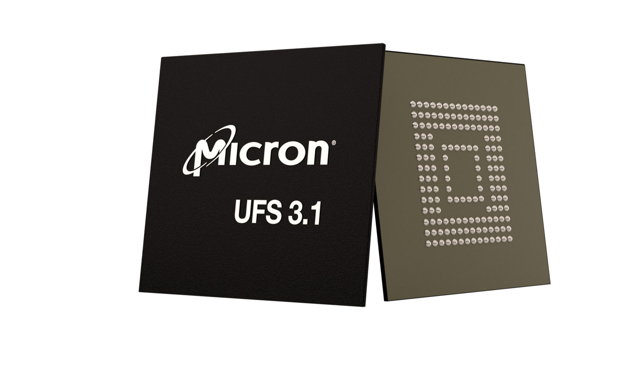
Product image of Micron UFS 3.1

Benefits

Facilitates exceptional battery life

The Micron UFS 3.1 devices require up to 83% less power during active use2 and 93% less power during sleep mode3 than other client SSD form factors. Power savings mean performance and extended battery life without thermal throttling.

Promotes creative PC designs that meet varied use cases

Unlike SSDs with M.2 form factors, a socket is unnecessary for the Micron UFS. Its thin 0.8mm z-height and 11.0 x 13.0mm profile provides 78% more PCB area than the smallest M.2 SSDs.4 Micron's UFS profile frees up space for more design flexibility in client devices.

Provides significantly higher performance than the e.MMC 5.1 standard

The Micron UFS 3.1 device Command Queue technology enables read and write commands simultaneously, resulting in random reads that are 4X faster than e.MMC and sequential writes that are 4X to 6X faster than e.MMC.5  Write speeds up to 1890 MB/s help prevent buffering when downloading files.

Based on a survey of public material at the time of this document’s publication.
The active-mode power consumption comparison: UFS –> VCCQ x ICCQ = 1.2V x 800mA = 960mW (max); 2450 M.2 SSD –> 5500mW (max); (5500 - 960)/5500 = 83%.
The sleep-mode power consumption comparison: UFS –> VCC x ICC = 2.5V x 80µA = 0.200mW (max); 2450 M.2 SSD –> 3mW (max); (3 - 0.200)/3 = 93%.
The "78% more PCB area" statement is due to a calculation based on the Micron UFS device's areal footprint of 143mm2 calculated from its x and y dimensions found in the Micron UFS FS194/195/196 data sheet and comparing the same areal footprint of 60mm2 calculated from the x and y dimensions found in the M.2 22x30 specification. (See https://www.snia.org/forums/cmsi/knowledge/formfactors#M2 for M.2 22x30 dimensions). (660-143)/660 = 78%.
Comparative random 4KB reads for e.MMC and UFS are 44KIOPS-53KIOPS and 180KIOPS-200KIOPS, respectively. Comparative sequential 512KB writes for e.MMC and UFS are 270 MB/s and 1200 MB/s–1890 MB/s, respectively.

Customer support

Need to get a hold of us? Contact our support teams as well as get contact information for our individual locations.

Search for, filter and download data sheets

Get in-depth information about product features, specifications, functionality, and more.

Order a Micron sample

Your online source for placing and tracking orders for Micron memory samples.

Downloads & technical documentation

Resources to help you design, test, build and optimize your innovative designs.